Combining n-MOS Charge Sensing with p-MOS Silicon Hole Double Quantum Dots in a CMOS platform
Published in Nano Letters
Ik Kyeong Jin, Krittika Kumar, Matthew J Rendell, Jonathan Yue Huang, Chris C Escott, Fay E Hudson, Wee Han Lim, Andrew S Dzurak, Alexander R Hamilton & Scott D Liles
Abstract
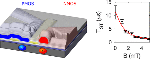
Holes in silicon quantum dots are receiving attention due to their potential as fast, tunable, and scalable qubits in semiconductor quantum circuits. Despite this, challenges remain in this material system including difficulties using charge sensing to determine the number of holes in a quantum dot, and in controlling the coupling between adjacent quantum dots. We address these problems by fabricating an ambipolar complementary metal-oxide-semiconductor (CMOS) device using multilayer palladium gates. The device consists of an electron charge sensor adjacent to a hole double quantum dot. We demonstrate control of the spin state via electric dipole spin resonance. We achieve smooth control of the interdot coupling rate over 1 order of magnitude and use the charge sensor to perform spin-to-charge conversion to measure the hole singlet–triplet relaxation time of 11 μs for a known hole occupation. These results provide a