Optimization of Silicon MOS Architecture for Self-Referenced Quantum Current Standard
Published in IEEE 2023 QCE
Ajit Dash, Steve Yianni, Jonathan Yue Huang, MengKe Feng, Fay Hudson, Andre Saraiva
Abstract
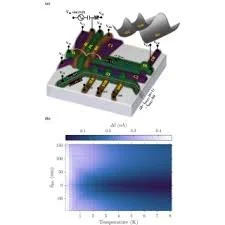
A semiconductor tunable barrier charge pump accurately generates electrical current by discretely transferring charges across a quantum dot. Practical implementation of this technology for realizing the revised quantum current standard requires robustness of the charge pumping fidelity to the control and measurement equipment used across various National Measurement Institutes. Here, we investigate an optimized device design to assess the charge pumping fidelity in-situ using electron counting technique. The architecture incorporates a previously measured silicon metal-oxide-semiconductor single-electron pump, which has been operated above the liquid helium temperature, and a double-island single-electron transistor as the charge sensor. Using TCAD simulation, we show that by optimizing the size of the top gates and the position of the quantum dots, the charge sensitivity can be improved by up to four times even above the liquid helium temperature.

