Holes in silicon are heavier than expected: transport properties of extremely high mobility electrons and holes in silicon MOSFETs
Available on arXiv
JP Wendoloski, J Hillier, SD Liles, M Rendell, Y Ashlea-Alava, B Raes, R Li, S Kubicek, C Godfrin, J Jussot, S Beyne, D Wan, Md M Rahman, S Yianni, KW Chan, FE Hudson, WH Lim, K De Greve, AS Dzurak, AR Hamilton
Abstract
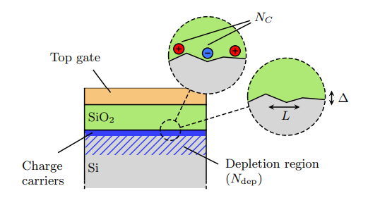
The quality of the silicon-oxide interface plays a crucial role in fabricating reproducible silicon spin qubits. In this work we characterize interface quality by performing mobility measurements on silicon Hall bars. We find a peak electron mobility of nearly in a device with a oxide layer, and a peak hole mobility of about in a device with oxide, the latter being the highest recorded mobility for a p-type silicon MOSFET. Despite the high device quality, we note an order-of-magnitude difference in mobility between electrons and holes. By studying additional n-type and p-type devices with identical oxides, and fitting to transport theory, we show that this mobility discrepancy is due to valence band nonparabolicity. The nonparabolicity endows holes with a density-dependent transverse effective mass ranging from to , significantly larger than the usually quoted bend-edge mass of . Finally, we perform magnetotransport measurements to extract momentum and quantum scattering lifetimes.